The Sensor That Sees in 3D: A Tiny Chip's Giant Leap for AI
- Resolution: 2,268 distinct zones (54x42 array) for high-resolution 3D imaging.
- Range & Accuracy: Detects objects from 5 cm to 9 meters with ~1% accuracy.
- Speed: Captures up to 100 frames per second.
Experts would likely conclude that the VL53L9 represents a significant advancement in accessible, high-resolution 3D sensing, poised to accelerate AI-driven automation across industries.
The Sensor That Sees in 3D: A Tiny Chip's Giant Leap for AI
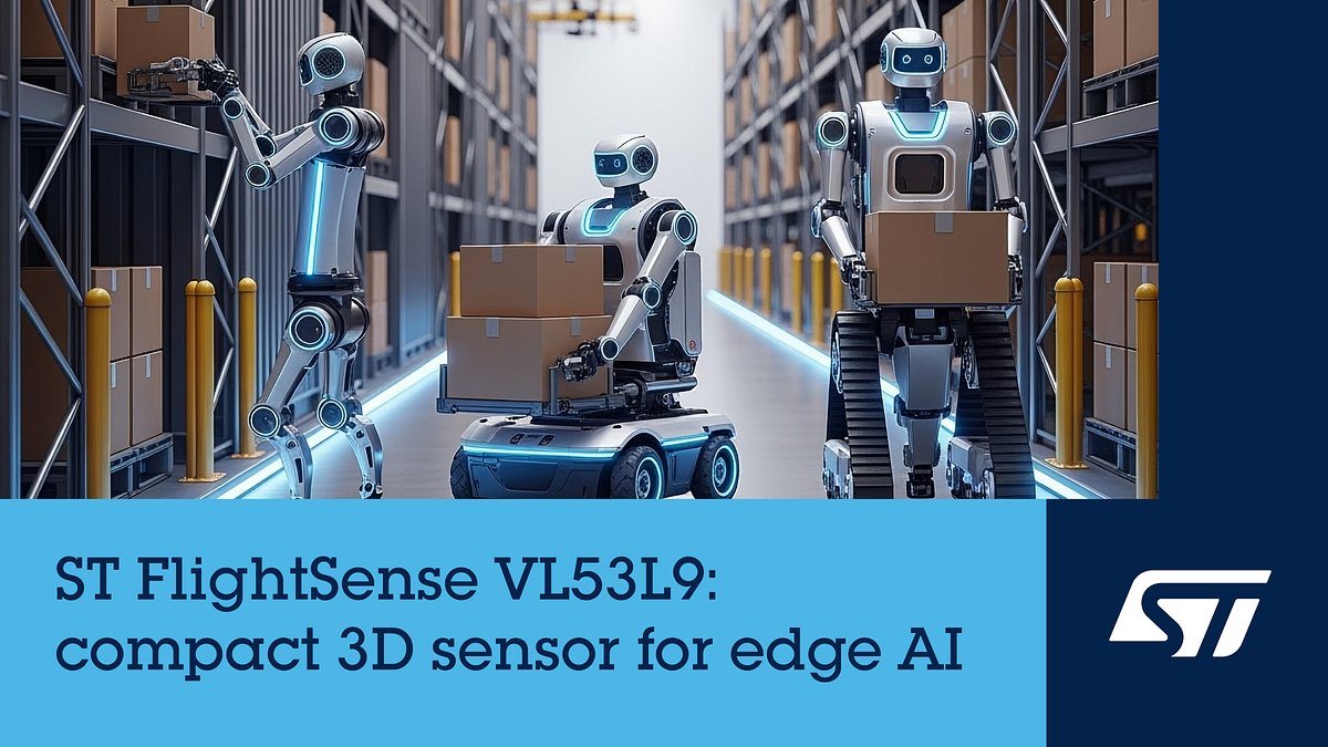
GENEVA, SWITZERLAND – June 22, 2026 – In a move that could fundamentally reshape how machines perceive the world, semiconductor giant STMicroelectronics today unveiled the VL53L9, a 3D LiDAR module smaller than a thumbnail. The announcement isn't just about another component; it represents a significant leap in making high-resolution spatial awareness accessible, affordable, and compact enough to embed into a new generation of intelligent devices, from warehouse robots to at-home healthcare monitors.
This tiny sensor promises to grant machines a nuanced, three-dimensional understanding of their surroundings, a capability that has long been the expensive and bulky province of autonomous vehicles and high-end surveying equipment. By shrinking the technology and integrating the intelligence directly onto the chip, STMicroelectronics is placing a powerful new tool in the hands of engineers and aiming to accelerate the arrival of the truly smart, autonomous systems we’ve been promised for years.
A New Benchmark for Machine Perception
The VL53L9 is what’s known as a direct Time-of-Flight (dToF) sensor. It works by emitting a pulse of invisible laser light and measuring the precise time it takes for photons to bounce off objects and return. By doing this across thousands of points, it builds a detailed “depth map” of a scene. While the principle isn't new, ST's execution sets a new competitive watermark.
The module projects a grid of 2,268 distinct zones (a 54x42 array) across a wide field of view, capturing a high-resolution 3D image at up to 100 frames per second. It can detect objects from as close as five centimeters to as far as nine meters away with an accuracy of around 1%. This combination of resolution, speed, and range is a potent cocktail, allowing a device to not only see that an obstacle is present but to understand its shape, size, and position with remarkable fidelity. This is the difference between a robot vacuum bumping into a table leg and one that navigates gracefully around a child’s scattered toys.
What truly distinguishes the VL53L9, however, is its all-in-one design. Historically, integrating such sensors has been a complex task for engineers, requiring separate processors, power management components, and painstaking calibration. STMicroelectronics has bundled all of this—the laser emitter, the sensor array, and the on-chip processing—into a single, calibration-free component. “By simplifying integration and reducing system complexity, we enable customers to accelerate the development of applications,” said Alexandre Balmefrezol, an Executive Vice President at STMicroelectronics, in a statement accompanying the launch.
This integrated approach is a direct challenge to the status quo. It democratizes access to advanced sensing, allowing smaller companies and startups to compete on a more level playing field. More importantly, because the depth data is processed directly on the chip, it can be fed to low-power microcontrollers, enabling sophisticated edge AI applications without requiring a connection to a power-hungry cloud server. This is critical for devices where speed, efficiency, and data privacy are paramount.
Beyond the Smartphone: LiDAR's Quiet Proliferation
For years, the most visible application of 3D sensing has been in flagship smartphones, subtly improving camera focus or enabling facial recognition. But the technology's potential extends far beyond our pockets. The market for 3D sensing is expanding rapidly into industrial, commercial, and healthcare environments, a trend the VL53L9 is perfectly positioned to capitalize on. According to market analyst firm Yole Group, “Higher resolution multizone dToF modules are now emerging as key enablers for this next wave of 3D sensing adoption.”
In the world of robotics, the module’s ability to detect small objects and map environments in real-time (a process called SLAM) is transformative. It allows autonomous mobile robots in warehouses to navigate dynamic, cluttered spaces with greater safety and efficiency. In industrial automation, its precision can be used for tasks like accurately measuring the volume of grain in a silo or ensuring packages are correctly stacked on a pallet, optimizing logistics and reducing waste.
Perhaps the most compelling applications are those with a direct human impact. In smart buildings, the VL53L9 can perform anonymous people counting and presence detection. Unlike a traditional camera, a depth sensor sees shapes and forms, not identifiable faces. This allows for the creation of smarter, more energy-efficient spaces that can adjust lighting and climate control based on occupancy, all while preserving the privacy of individuals within them—a crucial consideration in an era of mounting concern over digital surveillance.
Similarly, in healthcare, the technology offers a path to more dignified eldercare. A sensor like the VL53L9 can be used in fall detection systems, reliably monitoring a room for sudden changes in a person’s posture and alerting caregivers, without the intrusive eye of a video camera. It acts as a silent, respectful guardian, bridging the gap between safety and personal privacy.
STMicro's Strategic Pivot to an Integrated World
The launch of the VL53L9 is more than a product release; it's a clear signal of STMicroelectronics' strategic direction. As a recognized leader in the semiconductor industry, the company is moving from simply supplying components to providing integrated systems. Balmefrezol noted the launch reflects a strategy to “move beyond standalone sensors and deliver integrated sensing systems that support real-world edge AI.” It’s a high-stakes bet on a future where intelligence is distributed and embedded in the fabric of our environment.
This pivot is essential for maintaining a competitive edge. While ST holds a strong position, the 3D sensing space is crowded with formidable players like ams OSRAM and Infineon. By offering a solution that is not just technically powerful but also easy to implement, ST is aiming to capture the vast market of developers who need advanced capabilities without the associated engineering overhead.
Of course, widespread adoption is never guaranteed by a datasheet alone. The success of the VL53L9 will depend on the strength of the software ecosystem built around it and whether its cost can be justified at mass-market scale. But by targeting high-growth sectors and aligning its technology with macro trends like edge AI and privacy-centric design, STMicroelectronics is making a calculated play for the future of sensing.
As our devices gain the ability not just to compute, but to perceive, the line between tool and collaborator begins to blur. The tiny silicon eyes being forged in labs today will soon be looking out from the next generation of machines, and with them, they bring the potential for a world that is more efficient, responsive, and—if we are careful—more attuned to our human needs.
📝 This article is still being updated
Are you a relevant expert who could contribute your opinion or insights to this article? We'd love to hear from you. We will give you full credit for your contribution.
Contribute Your Expertise →