- 22nm Process: TetraMem's MLX200 platform is built on a commercial 22-nanometer process, one of the most advanced nodes for analog in-memory computing (IMC) technology.
- Multi-Level RRAM: The chip uses Resistive Random-Access Memory (RRAM) capable of representing thousands of distinct conductance levels, enabling high-density data storage and computation.
- 2026 Evaluation Kits: The company plans to ship evaluation kits to partners in the second half of 2026, accelerating market adoption.
Experts view TetraMem's MLX200 milestone as a significant advancement in energy-efficient AI hardware, offering a practical path to commercializing analog in-memory computing and addressing critical bottlenecks in modern computing.
TetraMem's Chip Milestone Signals a New Era for Energy-Efficient AI
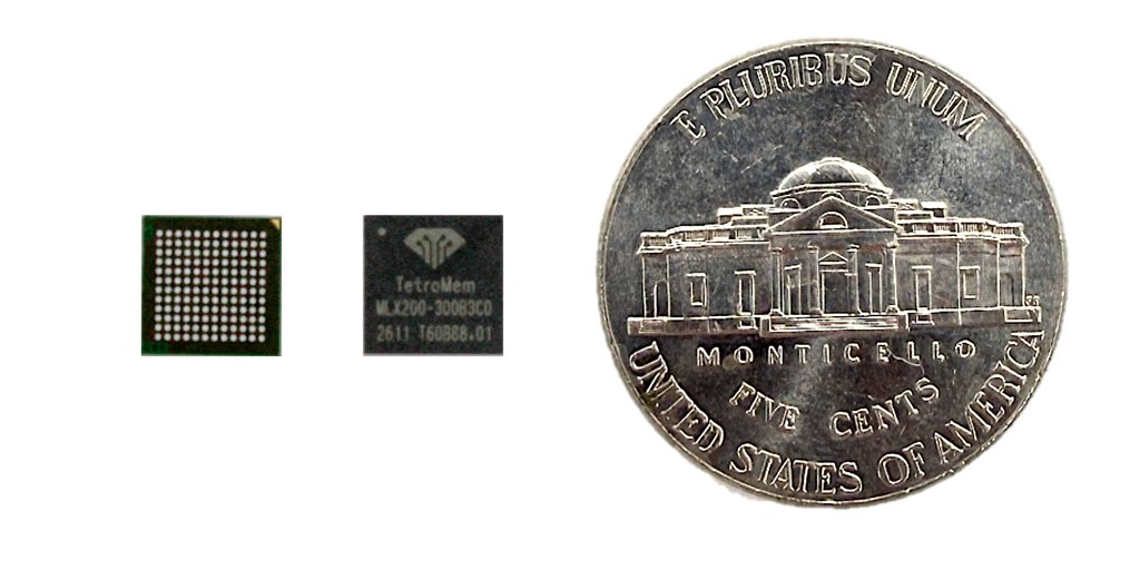
SAN JOSE, CA – May 16, 2026 – In a move that could fundamentally reshape the landscape of artificial intelligence hardware, Silicon Valley startup TetraMem has announced the successful production and initial validation of its MLX200 platform. The achievement marks a critical milestone: a multi-level analog in-memory computing (IMC) system-on-chip (SoC) built on a commercial 22-nanometer (nm) process, one of the most advanced nodes for this type of technology. This development directly confronts the most significant bottleneck in modern computing—the staggering energy cost of moving data—and charts a new course for building powerful, efficient AI into everything from wearable devices to industrial sensors.
For decades, computer architecture has been bound by the von Neumann model, where processing units and memory are physically separate. AI workloads, which require processing immense datasets, force a constant, energy-intensive shuttle of information between these two points. TetraMem’s technology bypasses this bottleneck by performing computation directly inside the memory itself. This analog IMC approach, now proven viable on a commercial manufacturing process with foundry giant TSMC, represents a significant step toward commercializing a technology that has long been a promising research concept.
A New Blueprint for AI Hardware
At the heart of TetraMem's innovation is Resistive Random-Access Memory (RRAM), a type of non-volatile memory that can store data by changing its electrical resistance. Unlike traditional digital memory that stores a '0' or a '1', TetraMem's RRAM devices are multi-level, capable of representing thousands of distinct conductance levels. This allows them to not only store vast amounts of information in a small physical space but also to perform complex mathematical operations—specifically the vector-matrix multiplications that are the lifeblood of neural networks—within the memory array itself.
The successful tape-out on TSMC's 22nm process is commercially significant. While novel chip architectures often debut on older, less complex nodes, proving the technology at 22nm demonstrates its compatibility with modern, high-volume CMOS manufacturing. This suggests a practical path to market, avoiding the “lab-to-fab” gap that stalls many hardware innovations. According to industry analysts, this move de-risks the manufacturing process and signals to potential customers and partners that the technology is ready for integration.
This milestone did not occur in a vacuum. It builds on a strong scientific foundation, including the company's previous MX100 platform on a 65nm process and landmark research published in prestigious journals. A 2023 Nature paper detailed the team's ability to achieve thousands of conductance levels in their memristors, and a follow-up in Science in early 2024 demonstrated how this could be leveraged for high-precision analog computing. “This milestone reflects years of close collaboration with our foundry partner TSMC and demonstrates the feasibility of bringing multi-level RRAM and analog in-memory computing from computing architecture breakthrough into advanced-node commercial silicon,” said Dr. Glenn Ge, Co-founder and CEO of TetraMem.
Navigating a Crowded and Competitive Field
TetraMem enters a fiercely competitive AI accelerator market, where startups and established giants are racing to build the next dominant architecture. However, its approach provides a distinct advantage in the burgeoning edge AI sector. While NVIDIA's powerful GPUs dominate the data center, their power consumption makes them unsuitable for most battery-powered devices. This has created an opportunity for innovators focused on performance-per-watt.
Several other startups are also targeting this space with novel architectures. Mythic, for instance, uses analog compute-in-memory but with more conventional flash memory, while companies like BrainChip and SynSense are pioneering neuromorphic, or brain-inspired, processors that excel at event-based tasks. TetraMem's use of multi-level RRAM, however, positions it as a leader in compute and memory density, a key factor for complex AI models.
To accelerate market adoption, the company is pursuing a shrewd dual-track commercialization strategy. It will offer the MLX200 as a standalone chip, with evaluation kits slated to ship to partners in the second half of 2026. Simultaneously, it is making its core multi-level RRAM technology available for licensing as an IP block. This allows other semiconductor firms to integrate TetraMem's analog compute engine directly into their own custom SoCs, significantly broadening its potential reach.
This strategy is backed by strong investor confidence. The company has secured funding from a notable list of strategic and financial investors, including semiconductor heavyweight SK Hynix, Shinhan Financial Group, and SAIC Capital. This backing not only provides financial runway but also validates the technology's commercial potential in the eyes of key industry players.
Unleashing Intelligence in Everyday Devices
The ultimate impact of the MLX200 and its successors will be felt in the devices we use every day. The platform's extreme energy efficiency is designed to enable continuous, complex AI workloads on power-constrained edge devices. This could unlock a new wave of 'always-on' intelligent applications that are currently infeasible.
In wearables, this technology could power smartwatches and fitness trackers that perform continuous biometric monitoring and analysis for days on a single charge. For audio applications, it could enable real-time noise cancellation and voice recognition that happens entirely on-device, improving privacy and responsiveness. In the vast Internet of Things (IoT) ecosystem, industrial sensors could use the MLX200 for local predictive maintenance analysis, and smart home devices could become truly intelligent without a constant connection to the cloud.
By moving AI inference from the cloud to the edge, TetraMem’s technology addresses critical concerns around latency, data privacy, and network dependency. For institutional investors and financial market analysts, this represents a pivotal shift in the semiconductor value chain, creating new opportunities for companies that can deliver the foundational hardware for a more distributed and intelligent world.
Dr. Ge believes this approach provides a “practical path to improving energy efficiency and scalability for next-generation AI systems.” As AI models continue to grow in complexity, the hardware that powers them must evolve. With its successful 22nm milestone, TetraMem has demonstrated that the future of AI computing may not just be faster, but fundamentally more efficient.