- $19 billion: South Korea's 2024 investment in semiconductor R&D, infrastructure, and talent development.
- 40% revenue surge: Tescan's projected 2025 revenue growth in the Asia-Pacific region.
- Over 50% of global market: Asia-Pacific's share of the semiconductor metrology and inspection market (2024).
Experts view Tescan's Seoul lab as a strategic investment that strengthens South Korea's semiconductor ecosystem, particularly in AI-driven memory and advanced chip packaging, while reinforcing international technological partnerships.
Tescan's New Seoul Lab Powers Korea's AI Semiconductor Ambitions
By Ruth Flores
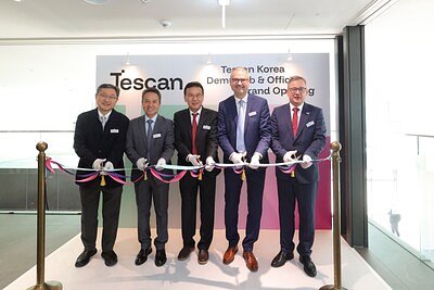
SEOUL, South Korea – March 20, 2026 – In a move that underscores South Korea's critical role in the global semiconductor race, Czech-based microscopy leader Tescan today inaugurated its upgraded Tescan Korea Demo Lab & Office in Seoul. The integrated facility is more than a new corporate office; it represents a strategic investment aimed directly at the heart of Korea's technological prowess: the development and production of next-generation AI-driven memory and advanced chip packaging.
The opening ceremony, attended by dignitaries including H.E. Ivan Jančárek, Ambassador of the Czech Republic to the Republic of Korea, and Jong-Seok Yeo, President of the Korea Society of Microscopy, signals the facility's importance. It is positioned as a crucial support hub for the nation's semiconductor giants and academic institutions, providing advanced tools and expertise needed to maintain a competitive edge in an increasingly complex industry.
Powering the AI Memory Revolution
South Korea's semiconductor ecosystem, home to titans like Samsung Electronics and SK Hynix, is the global epicenter for high-bandwidth memory (HBM), a critical component for powering artificial intelligence data centers. As these companies push the boundaries of technology with more complex, vertically stacked chip architectures, the challenges of ensuring reliability and pinpointing microscopic flaws have grown exponentially.
This is where the often-overlooked field of failure analysis (FA) becomes paramount. The new Tescan lab is equipped with advanced electron microscopy and focused ion beam (FIB) technologies that allow engineers to perform nanoscale investigations, essentially conducting autopsies on chips to identify defects mere atoms wide. This capability is vital for accelerating development cycles, improving manufacturing yields, and ensuring the reliability of chips that are foundational to the AI economy.
"APAC remains a key growth region for Tescan, and Korea is a strategic investment focus as the ecosystem scales AI memory capacity, including HBM, and advanced packaging," said Pavel Sustek, Chief Financial Officer at Tescan. "Our upgraded Seoul site is a direct investment in strengthening Tescan's customer-facing platform in Korea and in supporting semiconductor, materials science, and academic users."
The demand for these advanced FA solutions is surging. The Asia-Pacific region already commands over half of the global semiconductor metrology and inspection market, a sector valued at nearly USD 10 billion in 2024 and projected to grow significantly. As chip designs like Gate-All-Around (GAA) transistors and 3D packaging become standard, the need for sub-nanometer accuracy and automated, AI-enhanced analysis—the very services the Seoul lab will support—becomes non-negotiable.
A Strategic Foothold in a Competitive Market
Tescan's investment is also a calculated maneuver in the highly competitive semiconductor equipment market, where it vies with established players like Thermo Fisher Scientific and Hitachi High-Tech. While considered a challenger in terms of market share, the company is carving out a niche by focusing on integrated, workflow-focused solutions and product flexibility, a strategy that appears to be paying off. The company's semiconductor business in APAC accounted for nearly half of its global revenue in 2024, with projections for a 40% revenue surge in the region for 2025.
By establishing a direct presence in Seoul, the company is moving beyond being just a product vendor to becoming an embedded partner. The integrated demo lab and office create a hub for hands-on demonstrations, collaborative workflow validation, and intensive training sessions.
"By combining office and demo lab functions in one site, we have a stronger platform for customer discussions, workflow validation, and regional engagement," noted Sean Lee, Tescan's Managing Director for APAC. This customer-centric approach is crucial for building trust and tailoring solutions for the unique, high-stakes problems faced by Korean chipmakers.
The Seoul facility is the latest in a series of strategic expansions across Asia, following the establishment of subsidiaries in Taiwan and Singapore. This growing network demonstrates a clear corporate strategy to get closer to key customers and provide localized, high-touch support in the world's most dynamic semiconductor manufacturing hubs.
Fostering a National Semiconductor Ecosystem
The timing of Tescan's investment aligns perfectly with South Korea's national strategy. The government has declared the semiconductor industry a matter of national priority, launching initiatives like the "K-Chips Act" and committing over USD 19 billion in 2024 to support R&D, infrastructure, and talent development. This national push aims to solidify Korea's leadership against fierce international competition.
Tescan's new facility directly contributes to this national ambition. By providing local access to cutting-edge analysis tools, it helps Korean companies accelerate their R&D timelines for HBM and other advanced products. Furthermore, the lab's role extends into academia. The presence of the President of the Korea Society of Microscopy at the opening highlights a commitment to fostering collaboration between industry and research institutions. The facility will serve as a training ground for the next generation of engineers and scientists, helping to build the highly skilled workforce that is essential for long-term innovation and competitiveness.
Diplomacy Through Technology
The attendance of the Czech Ambassador lends a geopolitical dimension to the event, highlighting the deepening economic and technological ties between the Czech Republic and South Korea. This relationship has quietly blossomed into a significant partnership, with South Korea now standing as the Czech Republic's third-largest non-European trade partner and fourth-largest foreign investor.
While major Korean conglomerates like Hyundai and Nexen Tire have long had a major presence in the Czech automotive sector, the partnership is evolving into strategic high-tech fields. Recent collaborations include plans for a Czech-Korean robotics center in Prague and a landmark deal for Korea's KHNP to build new nuclear reactors in the Czech Republic. Tescan's investment in Seoul is another strong thread in this fabric of cooperation, showcasing how technology and business can fortify international alliances.
The new Seoul lab, therefore, is not merely a corporate milestone. It is a nexus where global business strategy, national technological ambition, and international diplomacy converge. It stands as a testament to the critical importance of the unseen work of failure analysis and a powerful enabler for the future of artificial intelligence being forged within South Korea's advanced semiconductor fabs.