- 11.7 Gbps per pin: Samsung's HBM4 achieves a processing speed of 11.7 Gbps per pin, with potential enhancements up to 13 Gbps, a 1.22x increase over HBM3E.
- 3.3 TB/s bandwidth: HBM4 delivers a maximum bandwidth of 3.3 TB/s per stack, a 2.7-fold increase compared to HBM3E.
- 40% power efficiency improvement: HBM4 offers a 40% improvement in power efficiency over its predecessor.
Experts would likely conclude that Samsung's early entry into HBM4 mass production positions it as a leader in the AI hardware race, offering significant performance and efficiency gains that will drive advancements in AI accelerators and data center technologies.
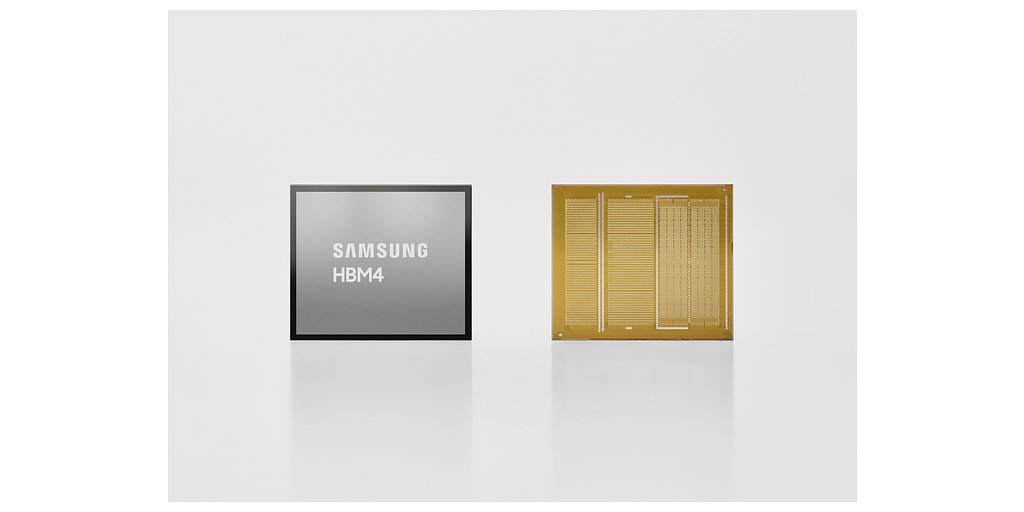
Samsung Ignites AI Race with Industry-First HBM4 Memory Shipment
SEOUL, Korea – February 12, 2026 – Samsung Electronics has fired the starting gun in the next leg of the artificial intelligence hardware race, announcing it has begun mass production and commercial shipment of HBM4, the next generation of high-bandwidth memory. The move, an industry first, positions the South Korean technology giant to capture a critical early lead in a market essential for powering the world's most advanced AI systems.
This announcement sends a clear signal to the market that the era of HBM4 has arrived, promising to unlock new levels of performance for AI accelerators, high-performance computing (HPC), and next-generation data centers.
A New Benchmark for Performance and Efficiency
At the heart of Samsung's announcement are performance metrics that represent a monumental leap over the current HBM3E standard. The new HBM4 memory delivers a staggering processing speed of 11.7 gigabits-per-second (Gbps) per pin, with the potential to be enhanced up to 13 Gbps. This is a 1.22x increase over the 9.6 Gbps peak speed of its HBM3E predecessor, effectively smashing through previous data processing ceilings.
The most significant figure for AI developers and hardware architects, however, is the total memory bandwidth. Samsung’s HBM4 boasts a maximum bandwidth of 3.3 terabytes-per-second (TB/s) per stack, a 2.7-fold increase compared to HBM3E. This dramatic expansion in data throughput is crucial for feeding the voracious data appetite of increasingly complex large language models (LLMs) and generative AI applications, mitigating the data bottlenecks that can throttle GPU performance.
This technological feat was achieved by taking a bold engineering path. Instead of iterating on existing designs, Samsung integrated its most advanced 6th-generation 10-nanometer class (1c) DRAM with a 4nm logic process for the base die. This integration of cutting-edge nodes allows for superior performance and efficiency.
“Instead of taking the conventional path of utilizing existing proven designs, Samsung took the leap and adopted the most advanced nodes like the 1c DRAM and 4nm logic process for HBM4,” said Sang Joon Hwang, Executive Vice President and Head of Memory Development at Samsung Electronics, in the company's press release. “By leveraging our process competitiveness and design optimization, we are able to secure substantial performance headroom.”
The company is initially offering HBM4 in 24GB and 36GB capacities using 12-layer stacking technology, with a roadmap that includes 16-layer stacks to achieve 48GB capacities in the future, directly addressing the need for larger memory pools in AI training.
Reshaping the High-Stakes Memory Market
Samsung's early entry into HBM4 mass production is a calculated strategic maneuver in the intensely competitive memory sector. The HBM market, though dominated by a triumvirate of Samsung, SK Hynix, and Micron, has seen SK Hynix gain significant ground in recent years with its HBM3 and HBM3E products. This announcement is a powerful countermove by Samsung to reassert its leadership.
While competitors are actively developing their own HBM4 solutions, their public timelines lag behind Samsung's claimed commercial availability. SK Hynix, a formidable rival, has announced plans to sample its HBM4 in 2026 with mass production slated for 2027. Micron, another key player, has been focused on ramping up its HBM3E production and has been less specific about its HBM4 mass production schedule.
By shipping commercial HBM4 products now, Samsung can secure early design wins with major customers and lock in lucrative, high-volume contracts for the next generation of AI hardware. This "first-mover" advantage is critical in a market where GPU and AI accelerator product cycles are planned years in advance.
The company's confidence is bolstered by its unique, vertically integrated manufacturing capabilities. The tight co-optimization between its Memory and Foundry businesses, a strategy it calls Design Technology Co-Optimization (DTCO), allows for streamlined production and superior quality control. This synergy, combined with one of the industry's largest DRAM production capacities, provides Samsung with a resilient supply chain to meet the projected explosion in HBM4 demand. The company anticipates its overall HBM sales will more than triple in 2026 compared to 2025, a forecast built on the back of this new technology.
Fueling the Next Wave of AI Innovation
The true impact of Samsung's HBM4 will be felt across the entire AI ecosystem, most notably by the designers of the world's most powerful chips. Companies like NVIDIA, AMD, and Intel, along with hyperscalers developing their own custom AI silicon, are the primary consumers of HBM. For them, this new memory is not just an incremental upgrade; it's an enabling technology.
The massive bandwidth increase allows for the creation of more powerful and efficient AI accelerators. Future GPUs and AI chips can be designed with wider memory interfaces to take full advantage of HBM4's capabilities, leading to faster training times for AI models and lower latency for inference tasks. This directly translates to more capable AI services, from more responsive chatbots to more complex scientific simulations.
For NVIDIA, whose data center GPUs have set the industry standard, securing a stable supply of the highest-performing HBM is paramount to maintaining its market dominance. For competitors like AMD and Intel, access to HBM4 is essential for creating competitive AI accelerators that can challenge the incumbent. The availability of commercial HBM4 will accelerate the product roadmaps of all these key players, likely influencing the architecture of AI chips set to be released in the coming years.
A Foundation for Sustainable, Scalable AI
Beyond raw performance, Samsung’s HBM4 addresses one of the most pressing challenges facing the AI industry: power consumption and thermal management. As data centers deploy tens of thousands of AI accelerators, the collective energy draw and heat generated have become major operational and environmental concerns.
Samsung's HBM4 achieves a 40% improvement in power efficiency compared to its HBM3E predecessor. This is accomplished through advanced low-power design solutions, including low-voltage Through Silicon Via (TSV) technology and optimized power distribution networks. This significant reduction in power consumption per gigabyte of data transferred helps lower the total cost of ownership (TCO) for data center operators.
Furthermore, the new memory enhances thermal management, improving heat dissipation by 30% and thermal resistance by 10%. Better thermal performance allows for denser server configurations and more reliable operation under the intense, continuous workloads typical of AI training. By tackling these efficiency and thermal challenges head-on, HBM4 provides a more sustainable foundation for the continued, massive scaling of AI infrastructure worldwide.
With the successful market introduction of HBM4, Samsung is already looking ahead. The company plans to begin sampling HBM4E—an even more advanced version—in the second half of 2026, with custom HBM solutions tailored to specific customer needs becoming available in 2027, ensuring the pipeline of memory innovation continues to flow as fast as the data it processes.
Topics & Related
Commodities & Materials
AI & Machine Learning
Cloud & Infrastructure
Semiconductors
Generative AI
Large Language Models
Artificial Intelligence
EBITDA
Revenue
Related Company Pulse