Flexcompute and Cadence Target AI's Data Bottleneck with Photonic Tool
- $2.86B to $28B: Silicon photonics market projected to grow from $2.86B in 2025 to $28B by 2034, a 30% CAGR. - 500x Faster: Flexcompute's GPU-accelerated simulations are up to 500 times faster than traditional CPU methods. - 70% Power Savings: Co-packaged optics (CPO) could reduce power consumption by up to 70% over traditional optics.
Experts agree that silicon photonics is essential for overcoming AI data center bottlenecks, and this collaboration between Flexcompute and Cadence significantly accelerates the design and optimization of photonic chips, addressing critical industry challenges.
Flexcompute and Cadence Unite to Break AI Data Center Bottlenecks
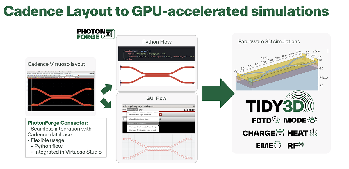
BOSTON, MA – March 19, 2026 – In a move set to accelerate the development of next-generation AI infrastructure, simulation specialist Flexcompute today announced the launch of its PhotonForge Connector for Cadence Virtuoso Studio. The integration embeds Flexcompute's powerful GPU-accelerated multiphysics simulation directly into Cadence's industry-leading design environment, promising to resolve a critical workflow chokepoint in the creation of advanced silicon photonic chips.
This collaboration arrives at a pivotal moment. As artificial intelligence models grow exponentially in complexity, the data centers that power them are straining against fundamental physical limits. The torrent of data flowing between processors has turned traditional copper interconnects into a significant bottleneck, throttling performance and consuming enormous amounts of power. Silicon photonics—the science of using light to transfer data on chips—is widely seen as the essential technology to overcome this barrier, and this new tool aims to make designing these intricate devices dramatically faster and more efficient.
The Silicon Photonics Imperative for AI's Future
The insatiable demand for computational power driven by generative AI and large language models (LLMs) is forcing a radical rethink of data center architecture. The industry is facing what experts call a "power wall" and a "communication bottleneck," where the energy required to move data is becoming as significant as the energy used for computation itself.
Silicon photonics addresses this challenge by replacing electrical wires with optical pathways, enabling data to travel at the speed of light with significantly lower power consumption and higher bandwidth. The market reflects this urgency. Industry analysts project the silicon photonics market to surge from approximately $2.86 billion in 2025 to over $28 billion by 2034, representing a compound annual growth rate of nearly 30%. This growth is largely fueled by the needs of AI data centers, which are rapidly migrating to 800G and 1.6T optical transceivers.
A key technology in this transition is co-packaged optics (CPO), which involves placing photonic components directly alongside processors and switches on the same package. "The industry's leading hyperscalers are heavily investing in co-packaged optics to address the growing I/O bandwidth demands of AI infrastructure," said Prashanta Kharel, PhD, Technology Strategist at Flexcompute. CPO promises to dramatically reduce latency and power consumption, with some estimates suggesting up to a 70% power saving over traditional pluggable optics. However, designing these highly integrated systems presents immense challenges.
Bridging the Critical Design-Simulation Gap
Creating effective silicon photonic devices requires precise modeling of complex, interacting physical phenomena, including electromagnetics, thermodynamics, and charge transport. Historically, the design process has been fragmented and inefficient. Engineers would create a device layout in a platform like Cadence Virtuoso Studio, then manually reconstruct that layout in a separate, specialized simulation environment to test its performance.
This disjointed workflow is not only time-consuming but also a frequent source of errors and inconsistencies between the intended design and the simulated model. Each iteration could take days or even weeks, severely limiting the ability to explore design variations and optimize for performance before committing to expensive manufacturing runs.
The new PhotonForge Connector for Cadence Virtuoso Studio eliminates this gap entirely. It establishes a seamless, two-way bridge between layout and analysis. Engineers can now automatically convert their photonic device layouts from the Cadence environment into simulation-ready 3D models with a single click. These models are then analyzed using Flexcompute's suite of GPU-accelerated solvers for FDTD, mode, charge, and heat simulations—processes that are up to 500 times faster than traditional CPU-based methods.
Crucially, the validated results, such as S-matrices that characterize the device's performance, are returned directly to the Cadence design environment. This integrated loop allows engineering teams to perform rapid parametric sweeps, run complex optimizations, and validate their designs against foundry-specific process design kits (PDKs), all without leaving their primary workspace.
A Strategic Alliance in a Competitive Landscape
This partnership is more than a simple product integration; it represents a strategic alignment in the highly competitive Electronic-Photonic Design Automation (EPDA) market. For Cadence, a dominant force in electronic design, the collaboration significantly strengthens its Virtuoso platform for the burgeoning photonics sector, helping it compete with comprehensive offerings from rivals like Synopsys and Ansys.
"The addition of Flexcompute to the Photonic Virtuoso Studio and Spectre Simulation ecosystem strengthens the capabilities available to our customers," noted Gilles Lamant, distinguished engineer and Virtuoso platform architect at Cadence. "This collaboration allows designers to access advanced simulation features directly within their photonic workflows, improving both productivity and validation accuracy."
For Flexcompute, the integration provides direct access to Cadence's vast user base, embedding its cutting-edge simulation technology into a workflow used by thousands of engineers worldwide. This move is central to Flexcompute's broader strategy of building an open engineering ecosystem where best-in-class tools work in concert. By partnering with established leaders, the company aims to accelerate innovation and lower the barrier to entry for designing complex, next-generation hardware.
The credibility of Flexcompute's technology is already established, with its simulation tools being used by key players in the semiconductor and photonics research landscape, including GlobalFoundries, Imec, AIM Photonics, and the Fraunhofer HHI. This new connector effectively productizes that advanced simulation power for a much wider audience of design engineers.
By streamlining one of the most difficult and time-consuming aspects of chip development, the collaboration between Flexcompute and Cadence provides a critical enabling tool for the entire AI industry. It empowers engineers to push the boundaries of what's possible with silicon photonics, ultimately paving the way for more powerful, efficient, and scalable AI systems that will define the next decade of computing.