- 20% reduction in system footprint, saving critical cleanroom space.
- 40% increase in internal capacity, integrating up to 14 bake/chill plates and two wet processing modules.
- 80% reduction in photoresist material use with spray coating technology.
Experts view the EVG120 as a breakthrough in semiconductor manufacturing, offering unmatched flexibility, efficiency, and precision for high-mix production, particularly in advanced packaging, MEMS, and other high-growth sectors.
EVG's Compact Powerhouse Aims to Reshape Chip Manufacturing
ST. FLORIAN, Austria – February 18, 2026 – By Thomas Moore
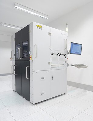
In a move poised to impact the production of next-generation electronics, semiconductor equipment supplier EV Group (EVG) today unveiled its next-generation EVG®120 automated resist processing system. The new platform is engineered to deliver the high-end performance of the company's larger systems but within an ultra-compact, highly flexible format, addressing a critical need for efficiency and versatility in the rapidly evolving semiconductor landscape.
The system is designed to support the fabrication of devices essential for booming markets like artificial intelligence, advanced automotive systems, and the Internet of Things (IoT). By integrating advanced metrology and process control into a smaller, more powerful platform, EVG is betting on a future where manufacturing agility is as crucial as raw processing power.
A Compact Powerhouse for High-Mix Manufacturing
The most striking feature of the new EVG120 is its mastery of paradox: it is substantially smaller yet significantly more powerful than its predecessor. The system's footprint has been reduced by over 20 percent, a critical advantage in the multi-billion-dollar cleanrooms where every square meter is prime real estate. Simultaneously, its internal capacity has increased by 40 percent, now integrating up to 14 bake/chill plates and two wet processing modules. This allows manufacturers to do more with less, boosting throughput per square meter and optimizing facility costs.
This design philosophy directly targets the growing segment of high-mix production. Unlike massive factories churning out a single type of chip in the millions, many of today's most innovative sectors—including MEMS, photonics, and advanced packaging—require facilities that can flexibly switch between different products, materials, and processes. The EVG120 is optimized for this environment, supporting a wide array of substrate sizes from 2 inches up to 200 mm and handling diverse materials from standard photoresists to specialized dielectrics.
EVG claims the system delivers performance on par with its widely adopted, larger EVG®150 platform. This achievement positions the EVG120 as a compelling option for not only high-volume manufacturers looking to optimize their line but also for research and development labs needing production-quality results on a smaller scale. The competitive landscape for such specialized equipment includes players like SUSS MicroTec, whose ACS200 Gen3 platform also targets advanced packaging and MEMS with proprietary coating technologies. The introduction of the EVG120's new capabilities underscores the intense innovation cycle in this specialized equipment segment.
Precision, Yield, and the Bottom Line
Beyond its compact form, the EVG120 introduces several breakthrough technologies aimed squarely at improving process control, which directly translates to higher manufacturing yields and a lower cost of ownership. Two features stand out: in-situ resist thickness measurement and Wafer Edge Exposure (WEE).
The new in-situ metrology allows the system to measure the thickness of the photoresist layer in real-time, with a range from a mere 50 nanometers up to 50 microns. This is akin to having a quality control inspector inside the machine during the process, providing immediate feedback that allows for automatic adjustments. This capability is crucial for preventing entire batches of expensive wafers from being ruined by an out-of-spec coating, dramatically reducing waste and improving overall yield.
Wafer Edge Exposure, another new addition, provides selective exposure at the wafer's edge. This creates a more precise and uniform boundary, which helps maximize the number of usable chips—or die—that can be harvested from each wafer. By eliminating edge-related defects, manufacturers can reclaim valuable silicon real estate that would otherwise be discarded.
These features are complemented by an enhanced high-viscosity dispense system, critical for the thick photoresists used in advanced packaging and MEMS. The system's closed-loop feedback ensures precise, repeatable coatings, which are fundamental to device reliability.
"The next-generation EVG120 platform leverages EV Group's decades of experience in photoresist and lithography processing to support the rapidly diversifying needs of our customers from R&D through volume production," stated Dr. Thomas Glinsner, corporate technology director at EV Group, in the company's announcement. He emphasized that the system delivers an "unmatched combination of coating and developing performance, throughput, flexibility and cost of ownership."
Fueling the Engines of Future Technology
The strategic importance of a tool like the EVG120 becomes clear when viewed through the lens of the markets it serves. Advanced packaging, a key enabler for the powerful processors used in AI and high-performance computing (HPC), is a market projected to soar past $70 billion by 2034. The versatility of the EVG120 in handling the complex structures and materials for these chiplet and 3D-stacked designs is a direct response to this demand.
Similarly, the MEMS market, which includes the microscopic sensors and actuators found in everything from smartphones and electric vehicles to medical devices, is on a trajectory to exceed $100 billion by the early 2030s. The EVG120's ability to coat surfaces with severe topographies and handle fragile substrates using technologies like its proprietary OmniSpray® system makes it a vital tool for this sector's continued miniaturization and innovation.
This trend continues across other target applications. The image sensor market, driven by automotive ADAS systems and ubiquitous smartphone cameras, is forecast to grow to over $70 billion by 2035. Photonics, the science of light that underpins our global data networks and is enabling new medical technologies, is a trillion-dollar industry. The EVG120's adaptability makes it a foundational piece of manufacturing equipment capable of supporting the diverse requirements of all these high-growth fields.
A Nod to Sustainability and Efficiency
In an industry known for its high energy and resource consumption, the EVG120 also incorporates features that address the growing demand for sustainable manufacturing. The new 'Stand-by Mode' reduces energy consumption during idle periods, a feature that supports compliance with the SEMI E167 standard for energy-saving equipment. This allows fabrication plants to better manage their energy footprint and reduce operational costs.
This focus on efficiency extends to material usage. EVG's established technologies, such as the CoverSpin™ bowl design and OmniSpray® conformal coating, are designed to minimize the consumption of expensive photoresists and other chemicals. For instance, spray coating can reduce material use by 80 percent or more compared to traditional methods for certain applications. This commitment to reducing waste, combined with the new system's energy-saving features, reflects a broader industry trend toward more environmentally responsible manufacturing. This holistic approach, blending performance with responsibility, signals a new era for flexible semiconductor fabrication.