- 16nm Process Advantage: Up to 65% higher speeds or 70% lower power consumption compared to 22nm nodes.
- Market Potential: Edge AI chip market projected to reach $140 billion by 2032.
- Integration Benefits: Fully integrated Bluetooth Low Energy (BLE) subsystem reduces system complexity and cost.
Experts would likely conclude that EMASS's 16nm AI chip represents a significant advancement in edge computing, offering substantial power and performance improvements that position it as a strong contender in the competitive ultra-low-power AI market.
EMASS Unveils 16nm AI Chip to Power Next-Gen Smart Devices
LOS ANGELES, CA – December 17, 2025 – EMASS, the semiconductor subsidiary of Nanoveu, today announced a significant leap forward in edge computing. The company’s next-generation ECS-DoT System-on-Chip (SoC), built on an advanced 16-nanometer (nm) process, has entered the final stages of development and is heading for fabrication at industry giant TSMC. This move signals a pivotal moment for always-on artificial intelligence, promising to embed more powerful, faster, and more efficient intelligence into a new wave of consumer and industrial devices.
The new chip builds upon the company's existing 22nm platform, aiming to solidify its leadership in the ultra-low-power Edge AI market. By migrating to a more advanced manufacturing process and integrating a suite of new features, EMASS is positioning itself to capture the growing demand for on-device processing in an increasingly connected world.
A New Era for Always-On Intelligence
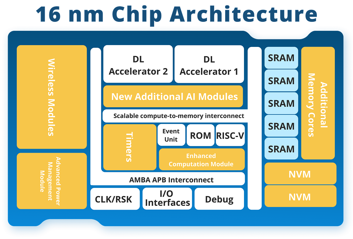
The transition from a 22nm to a 16nm process node is more than an incremental update; it represents a fundamental enhancement in capability. TSMC's 16nm FinFET technology is known to deliver substantial gains, potentially offering up to 65% higher speeds or 70% lower power consumption compared to older nodes. For EMASS, this translates into a powerful platform for applications where battery life and performance are paramount.
"With the 16nm ECS-DoT, we reach a defining moment for EMASS as we scale our architecture into new classes of applications demanding more intelligence, more speed and even lower power," said Mark Goranson, CEO of EMASS. "By migrating to 16nm, we've unlocked all new use-cases and identities that allow customers to push machine learning to the absolute edge, without sacrificing battery life or form-factor constraints."
Beyond the process shrink, the new SoC is packed with integrated features designed to reduce system complexity and cost for device manufacturers. A key enhancement is the fully integrated Bluetooth Low Energy (BLE) subsystem, which eliminates the need for a separate wireless IC. This not only shrinks the circuit board footprint but also lowers the bill-of-materials, a critical factor for mass-market devices like wearables and smart sensors.
Further bolstering its AI credentials, the chip includes expanded on-chip SRAM to support larger and more complex AI models, a dedicated object-detection accelerator to offload demanding vision workloads, and an integrated floating-point unit (FP16/FP32). This combination is engineered to accelerate AI inference for vision, audio, and sensor data directly on the device, enabling more capable always-on intelligence without constantly communicating with the cloud.
Navigating a Crowded Edge AI Battlefield
EMASS is entering a fiercely competitive landscape. The Edge AI chip market, projected to swell to over $140 billion by 2032, is a battleground for established giants and specialized startups alike. Competitors like Syntiant, with its power-sipping Neural Decision Processors, and Renesas, with its high-performance microcontrollers, are also vying for dominance in the ultra-low-power segment.
However, EMASS's 16nm ECS-DoT brings a compelling set of differentiators. The move to the 16nm node provides an immediate power and performance advantage over rivals still utilizing 22nm or larger processes. Furthermore, the high level of integration—combining core processing, AI acceleration, and wireless connectivity on a single die—presents a strong value proposition for developers looking to simplify design and shorten time-to-market.
The company's use of a RISC-V architecture, an open-source instruction set gaining traction for its flexibility and efficiency, could also provide a competitive edge in cost and customization. This strategic combination of advanced manufacturing, thoughtful integration, and a modern architecture positions the ECS-DoT as a formidable contender for next-generation IoT, drone, and medical device designs.
From Atoms to Apps: A Strategic Play for Nanoveu
The development of the 16nm chip is a cornerstone of parent company Nanoveu's broader "Atoms-to-Apps" strategy. This philosophy centers on creating fundamental technologies—the "atoms" like advanced silicon—that enable a wide array of end-user applications. For Nanoveu, which also develops glasses-free 3D display technology and other advanced materials, the EMASS SoC is a critical engine for powering intelligent human-machine experiences at the edge.
"This next generation of ECS-DoT represents a significant architectural advance for EMASS, bringing together always-on intelligence, deeper on-chip resources and higher levels of integration within a single ultra-low-power Edge AI platform," stated Dr. Mohamed Sabry, founder and CTO of EMASS. He emphasized that extending the architecture to support more demanding workloads without sacrificing efficiency strengthens the company's leadership and expands what is possible for its partners.
For Nanoveu (ASX: NVU), a successful launch of the 16nm chip could have a significant financial impact. Tapping into the high-growth markets for industrial IoT—projected to exceed $1.6 trillion by 2030—and AI-enabled medical devices offers a substantial revenue opportunity. A positive market reception could bolster investor confidence and validate the company's long-term vision of building a diversified technology portfolio.
Empowering Developers and Accelerating Innovation
Perhaps one of the most critical features of the new SoC is its developer-centric design. EMASS has ensured complete software and workflow compatibility with its existing 22nm ECS-DoT family. This seamless upgrade path is a powerful incentive for engineering teams, as it allows them to leverage their existing code and development tools while scaling up to more demanding AI workloads.
This compatibility drastically reduces the engineering effort and cost associated with migrating to a new hardware platform. Developers creating products for the booming AI-powered drone market, which is expected to surpass $60 billion by 2032, or for intelligent healthcare wearables, can integrate more advanced features without a complete product redesign. The result is a faster cycle of innovation, allowing new and improved smart devices to reach the market more quickly.
With the chip now heading for GDS sign-off and tape-out, the next steps involve the complex process of fabrication, testing, and yield optimization at TSMC. The journey from tape-out to volume production typically takes many months and must navigate a global semiconductor supply chain fraught with geopolitical tensions and logistical hurdles. Nonetheless, the milestone represents a clear and determined step toward delivering a new class of intelligence to the very edge of our digital world.