- 700 watts of heat per chip generated by next-gen AI accelerators and GPUs, threatening performance.
- 3,600 watts per device projected by 2027 for top-tier AI accelerators, pushing infrastructure limits.
- 40-50% of data center energy consumed by cooling systems, a figure set to rise with AI adoption.
Experts agree that heavy-copper PCBs represent a foundational hardware-level solution to AI's thermal management crisis, enhancing performance, reliability, and energy efficiency in data centers.
Cooling AI's Fever: Heavy-Copper PCBs Tackle a Critical Bottleneck
SHENZHEN, China – January 19, 2026 – As the artificial intelligence revolution accelerates, the very hardware powering it is hitting a wall of fire. Next-generation AI accelerators and GPUs, the engines of modern machine learning, now frequently generate over 700 watts of heat per chip—a thermal load that threatens to throttle performance and halt progress. Addressing this critical physical limitation, specialized manufacturer PCBAIR has announced a significant upgrade to its manufacturing process, introducing advanced heavy-copper printed circuit boards (PCBs) designed to tame the heat and unlock AI's future potential.
The announcement positions the humble PCB, often seen as a passive component carrier, as an active and vital part of the solution to one of the tech industry's most pressing challenges. By enabling the board itself to act as a highly efficient heat sink, the innovation promises to enhance performance, improve reliability, and potentially lower the staggering energy costs associated with cooling AI data centers.
The AI Thermal Bottleneck
The computational thirst of AI is creating a thermal crisis. As models grow in complexity, the chips running them are becoming exponentially more power-hungry. Industry projections show that top-tier AI accelerators could demand up to 3,600 watts per device by 2027, pushing current infrastructure to its breaking point. This intense power consumption translates directly into heat, creating power densities in server racks that can exceed 120kW—far beyond what traditional air-cooling methods can effectively manage.
When a chip overheats, it triggers a self-preservation mechanism known as “thermal throttling,” automatically reducing its clock speed to cool down. For data centers running multi-trillion-parameter AI models, this slowdown is not just an inconvenience; it represents a direct loss of computational power, wasted energy, and a significant financial impact. Furthermore, sustained high temperatures degrade components, shortening the lifespan of expensive hardware and compromising system reliability.
This challenge has made thermal management a primary focus for system architects. Cooling systems already account for a staggering 40-50% of a data center's total energy consumption, a figure that is set to balloon as AI adoption grows. Without foundational improvements at the hardware level, the escalating energy demands and environmental footprint of AI could become unsustainable.
A Foundational Fix at the Board Level
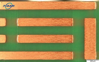
PCBAIR’s solution tackles this problem at its source. The company has upgraded its production lines to support the precision fabrication of heavy-copper PCBs, with copper weights of up to 10 ounces (approximately 350µm) on both inner and outer layers. This is a substantial increase over the standard 1-2 ounce copper layers found in most consumer electronics. The thicker copper traces can handle far higher electrical currents with lower resistance, reducing I²R losses—heat generated by the flow of electricity itself—and more importantly, they can spread and dissipate heat away from critical components like GPUs and voltage regulators.
“The PCB has evolved from a passive carrier to an active component of the thermal solution,” said Victor Zhang, CTO of PCBAIR, in the company's announcement. The true difficulty, he explained, lies not just in applying thick copper, but in manufacturing it with precision.
Heavy-copper fabrication is notoriously challenging. The chemical etching process required to create circuits can lead to “undercutting,” where traces become narrower than designed, compromising electrical performance. Another common defect, “resin starvation,” occurs during lamination, where gaps in the thick copper layers are not properly filled, creating micro-voids that can lead to board failure.
PCBAIR states its upgraded process overcomes these hurdles using advanced differential etching compensation and vacuum-assisted resin filling. “The real challenge with heavy copper isn't just plating thickness; it is achieving straight sidewalls to ensure electrical performance,” Zhang noted. These techniques ensure the high-current capacity engineers need without the delamination risks that have plagued thick-copper boards in the past.
Advanced Engineering for Extreme Reliability
To meet the stringent demands of Tier-1 data centers and the automotive industry, PCBAIR has integrated several key technologies into its heavy-copper offerings. One of the most significant is Embedded Copper Coin Technology. This process involves integrating solid copper slugs, or “coins,” directly into the PCB cutouts beneath major heat-generating components. These coins create a highly efficient vertical thermal path, pulling heat directly from a chip or voltage regulator and transferring it to a chassis or larger heat sink, bypassing the PCB's standard FR-4 substrate, which is a poor thermal conductor.
This approach complements the board's enhanced horizontal heat-spreading capabilities, creating a comprehensive thermal management system within the PCB itself. The company also ensures its boards are compatible with High-Tg (high glass transition temperature) laminates, materials specifically designed to withstand the rigorous and repeated thermal cycles common in data center environments without losing their structural integrity.
To validate these enhancements, the company implemented a rigorous testing regimen. Internal reports indicate that prototype boards successfully passed 1,000 cycles of thermal shock testing, fluctuating between -40°C and +125°C with zero continuity failures. This demonstrates the robustness of the interconnects and Plated Through Holes (PTH), providing the high degree of reliability required for mission-critical AI infrastructure.
Strategic Implications for the Future of Computing
This technological advancement marks a strategic expansion for the Shenzhen-based manufacturer, moving its focus toward the high-stakes infrastructure powering the global AI and automotive industries. By providing a robust, board-level solution to thermal management, the company is positioning itself as a key enabler in the high-performance computing supply chain.
More efficient heat dissipation at the PCB level allows for greater computing density, enabling data center operators to pack more processing power into each server rack. This not only maximizes the use of physical space but also contributes to greater energy efficiency by reducing the burden on external cooling systems. As data centers increasingly adopt advanced solutions like direct-to-chip liquid cooling and full immersion cooling, having a thermally efficient PCB becomes even more critical, as it enhances the effectiveness of the entire system.
PCBAIR's innovation underscores a broader trend where every component in the hardware stack is being re-engineered to support the extreme demands of artificial intelligence. As the industry continues to push the boundaries of what's computationally possible, foundational technologies like the printed circuit board are proving to be more critical than ever in paving the way forward.